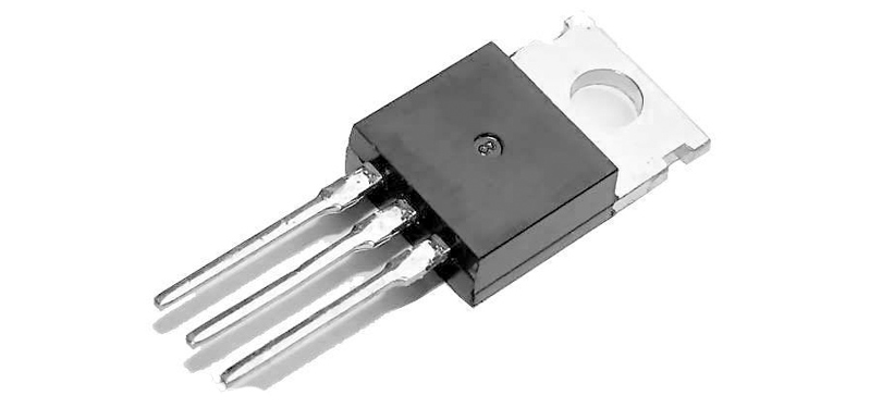

What is the difference between when we do the circuit design and the triode and MOS tube are used as switches?
Nature of the work:
1, the triode with current control, MOS tube is a voltage control.
2, the cost of the problem: the triode is cheap, MOS tube is expensive.
3, power consumption problem: the triode loss is large.
4, drive capability: MOS tube is commonly used to power switch, and high current place switch circuit.
In fact, the triode is relatively cheap, easy to use, and is commonly used in digital circuit switching control.
MOS tubes are used in high frequency, high speed circuits, high current applications, and where the base or drain control current is sensitive.
Generally speaking, in low-cost applications, triodes are considered for common applications, and MOS tubes are not considered.
In fact, it is wrong to say that current control is slow and voltage control is fast. To understand the way in which bipolar and MOS transistors work, you can understand. The triode is operated by the motion of the carrier. Taking the npn tube emitter follower as an example, when the base is not applied with voltage, the pn junction composed of the base region and the emitter region is blocked by multiple ions (the base region is a hole). The emission region is an electron diffusion motion. At this pn junction, an electrostatic field (ie, a built-in electric field) directed from the emitter region to the base region is induced. When the base is applied with a positive voltage, the base region is directed to the emitter region. When the electric field generated by the applied voltage of the base is greater than the built-in electric field, the carriers (electrons) in the base region may flow from the base region to the emitter region. The minimum value of this voltage is the forward conduction voltage of the pn junction (it is generally considered in engineering) 0.7v). However, at this time, there is a charge on both sides of each pn junction. At this time, if the collector-emitter is positively charged, the electrons in the emitter region move toward the base region under the action of the electric field (actually, the opposite direction of the electron moves. ), because the width of the base region is small, electrons easily cross the base region to reach the collector region, and recombine with the holes of the PN here (near the collector), in order to maintain the balance, under the action of the positive electric field, the collector region The electron accelerates the movement of the outer collector, while the cavity moves at the pn junction, a process similar to an avalanche process. The collector's electrons return to the emitter through the power supply, which is how the transistor works. When the triode is working, both pn junctions will induce a charge. When the switch is in the on state, the triode is in a saturated state. If the triode is turned off at this time, the charge induced by the pn junction should be restored to equilibrium. This process takes time. The MOS transistor works differently and does not have this recovery time, so it can be used as a high-speed switch.
(1) The field effect transistor is a voltage control element, and the transistor is a current control element. In the case where only a small current is allowed from the signal source, the FET should be used; and when the signal voltage is low and the current is taken from the signal source, the transistor should be selected.
(2) FETs use majority carriers to conduct electricity, so they are called unipolar devices, and transistors have most carriers and are also conductive with minority carriers. It is called a bipolar device.
(3) The source and drain of some FETs can be used interchangeably. The gate voltage can also be positive or negative, and the flexibility is better than that of the transistor.
(4) The FET can work under very low current and very low voltage conditions, and its manufacturing process can easily integrate many FETs on one silicon chip, so the FET is in large scale integrated circuit. It has been widely used.
(5) Field effect transistors have the advantages of high input impedance and low noise, and are therefore widely used in various electronic devices. In particular, the field effect tube is used as an input stage of the entire electronic device, and it is possible to obtain a performance that is difficult to achieve with a general transistor.
(6) The FET is divided into two types: junction type and insulated gate type, and the control principle is the same.


Add:Innovation Workshop F3, No. 2016 Feiyue Avenue, Innovation Zone,Jinan
E-Mail:Export@hfzt.net
E-Mail:Export2@hfzt.net
Mob:+86-18678883083
Phone:+86-531-80997880


Jinan HFZT Electronic Co.,Ltd. © 2007-2017 HFZT.NET All Rights Reserved.